

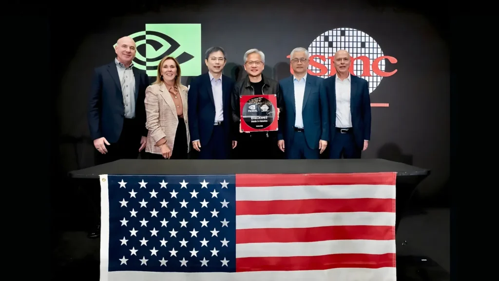
NVIDIA and TSMC have officially produced the first Blackwell AI chip wafer in the United States, marking a historic leap in domestic chipmaking. The wafer was manufactured at TSMC’s Fab 21 in Phoenix, Arizona, and celebrated on October 17, 2025, with NVIDIA CEO Jensen Huang and TSMC executives signing it to commemorate the milestone.
Blackwell Wafer Milestone
The Blackwell wafer, fabricated on TSMC’s 4N process (a custom 4nm-class node developed for NVIDIA), represents the first U.S.-made version of what is arguably the most advanced AI chip architecture in the world. It contains approximately 208 billion transistors and serves as the foundation for NVIDIA’s B300 series GPUs, designed to power next-generation generative AI models and datacenter workloads.
Strategic and Political Significance
The event highlights President Trump’s reindustrialization agenda, emphasizing the push to bring semiconductor manufacturing back to America. Huang called it “the single most important chip being manufactured in the U.S.,” symbolizing a major achievement in strengthening the domestic AI technology stack and reducing dependency on Asian supply chains.
Ongoing Collaboration and Next Steps
Although the wafers are fabricated domestically, final assembly and advanced packaging using TSMC’s CoWoS (Chip-on-Wafer-on-Substrate) process will still occur in Taiwan. Plans are underway for Amkor Technology to begin U.S.-based CoWoS packaging by 2026, which will bring the entire chip production pipeline closer to completion in America.
Broader AI Infrastructure Impact
NVIDIA’s domestic wafer production coincides with its $500 billion investment commitment to building AI infrastructure in the U.S. over the next four years, involving partnerships with TSMC, Foxconn, and major U.S. tech firms. This move is expected to boost job creation, strengthen supply resilience, and enhance U.S. competitiveness in global AI chip production.
Also Read: Andhra Pradesh aims Davos-style Partnership summit after Google’s $15B landmark investment